
The Complete Guide to Semiconductor Manufacturing
From smartphones and computers to vehicles and medical equipment, semiconductors are the backbone of almost every electronic device. With technological advancements and the rapid expansion of the electronics industry, semiconductor demand has surged globally.
If you’re interested in entering this high-growth industry, you must understand the semiconductor manufacturing process.
This guide outlines the essential phases of semiconductor manufacturing, key technologies, and the growing role of India in this critical industry.
Understanding the Basics of Semiconductors
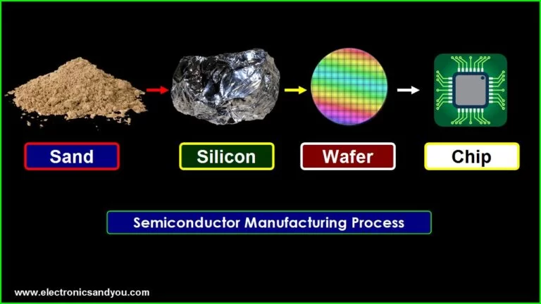
Semiconductors are materials that have electrical conductivity between conductors (like copper) and insulators (like glass). Silicon is the most commonly used material in semiconductor manufacturing because of its abundance and excellent conductive properties.
© Electronics Tutorial Website
These devices are used to create integrated circuits (ICs) and microchips that control the functioning of various electronic gadgets. The complexity of semiconductor manufacturing lies in the need for precision, cleanliness, and advanced technology.
Key Phases in Semiconductor Manufacturing
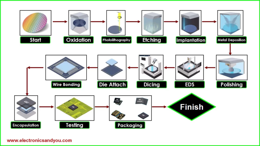
1. Wafer Production
The process begins with the production of silicon wafers. High-purity silicon is melted and formed into cylindrical ingots, which are sliced into thin wafers. These wafers act as the substrate on which semiconductor devices are built.
Precision in this phase is critical, as the wafers must have an ultra-smooth surface to ensure uniformity during subsequent steps. Advanced machinery is used to polish the wafers, making them ready for further processing.
2. Photolithography
Photolithography is a crucial step where patterns are transferred onto the wafer using light and a photosensitive material called photoresist. The wafer is coated with photoresist, exposed to ultraviolet (UV) light through a mask, and then developed to create a pattern.
This process allows the creation of intricate circuit designs on a microscopic scale. As technology evolves, extreme ultraviolet (EUV) lithography is being adopted to achieve even smaller feature sizes, enabling higher performance chips.
3. Etching and Doping
Once the pattern is created, etching removes unwanted material from the wafer. This can be done using either a wet chemical process or a dry plasma process, depending on the required precision.
Doping introduces impurities into the silicon to modify its electrical properties. This is achieved by exposing the wafer to dopant gases or ion beams, creating regions of positive (p-type) and negative (n-type) conductivity.
4. Deposition of Thin Films
Various thin films are deposited on the wafer to form the different layers of the semiconductor device. Techniques such as chemical vapor deposition (CVD) and physical vapor deposition (PVD) are used to apply these layers with precision.
Each layer plays a distinct role in the final chip’s operation, and any deviation in thickness or uniformity can affect performance.
5. Chemical Mechanical Planarization (CMP)
After deposition, the wafer surface may become uneven. CMP smoothens the surface by combining chemical and mechanical polishing techniques.
The purpose of this step is to ensure that subsequent layers are applied uniformly, protecting the integrity of the chip design.
6. Packaging and Testing
Once the fabrication process is complete, the individual chips are cut from the wafer, packaged, and tested. Packaging protects the chip from physical damage and environmental factors while providing the necessary connections to external devices.
Testing ensures that only fully functional chips reach the market. Each chip undergoes rigorous quality control to detect defects and ensure compliance with performance standards.
Key Technologies in Semiconductor Manufacturing
1. Cleanroom Environment
Semiconductor manufacturing requires an ultra-clean environment to prevent contamination.
Cleanrooms with controlled temperature, humidity, and air quality are essential to maintain the integrity of the manufacturing process.
2. Automation and Robotics
The complexity of semiconductor production makes automation indispensable. Robots are used for wafer handling, lithography, and inspection tasks, ensuring precision and minimizing human error.
3. Advanced Metrology Tools
Accurate measurement and inspection are crucial at every stage of manufacturing. Metrology tools such as scanning electron microscopes (SEMs) and atomic force microscopes (AFMs) are used to inspect patterns and layer thickness.
Challenges in Semiconductor Manufacturing
Despite technological advancements, semiconductor manufacturing faces several challenges:
- High Capital Investment: Establishing a semiconductor fabrication plant (fab) requires billions of dollars in investment due to the need for advanced equipment and cleanroom facilities.
- Rapid Technological Changes: The semiconductor industry evolves rapidly, with new technologies emerging every few years. To remain competitive, companies need to invest continuously in research and development.
- Supply Chain Dependencies: The production process depends on a complex global supply chain. Any disruption in the supply of raw materials or equipment can significantly impact production timelines.
India’s Role in the Semiconductor Industry
 © Wright Research & Capital Pvt Ltd
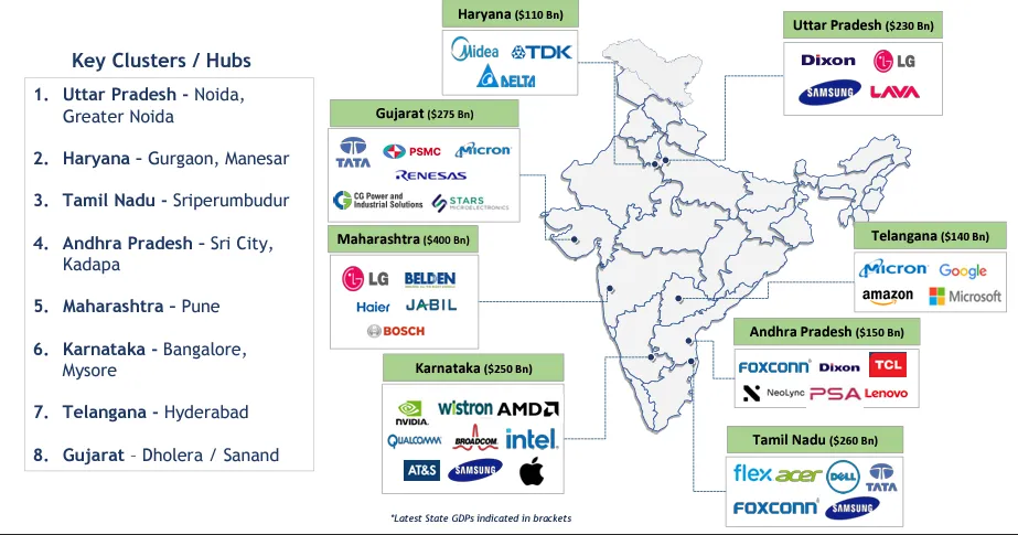
India is emerging as a key player in the global semiconductor industry. Government initiatives such as the “Make in India” campaign and the Production Linked Incentive (PLI) scheme have attracted significant investment in semiconductor manufacturing.
Several multinational corporations have expressed interest in setting up semiconductor fabs in India. The country’s large talent pool, robust IT infrastructure, and growing electronics market make it an attractive destination for semiconductor manufacturing.
VMS Consultants previously worked on many large-scale industrial facility projects, showcasing our expertise in engineering and project management for high-tech industries.
Read more – India’s Rise as a Global Semiconductor Manufacturing Hub | IBEF
Conclusion
Semiconductor manufacturing is a complex yet rewarding process that demands precision, advanced technology, and significant investment.
With more than six decades of experience in setting up industrial facilities, VMS Consultants offers end-to-end engineering, architecture, and project management services.
VMS Consultants is one of the best project management consultants in Gujarat, providing comprehensive solutions. Get in touch with us to learn more!